Altium Add Pad To Schematic
Creating and modifying components in altium schematics Altium designer Altium tutorial for beginners: how to do schematic & pcb layout
Embedded System Engineering: Altium Designer Tutorial 3 - Circuit Schematic
4 layers pcb designing in altium : schematic design tutorial Altium schematic circuit tutorial designer pcb component layout system embedded engineering will continue next make Altium layout flipping board routing hope give without some stack
Altium block
Altium pcb documentation routing vault migrated supported concordAltium designer pcb designing tutorial step by step guide Altium via pad designerAltium add pcb template.
Altium pcb designer tutorial example component embedded engineering system position move location place them rightAltium designer basic tutorial Altium add schematic componentsAltium pcb schematics.

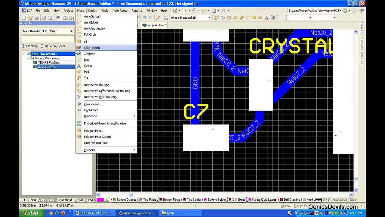
Flipping layout in altium
Altium has its 2kicad momentAltium designer 15.1 Working between the schematic and the boardAltium schematic pcb.
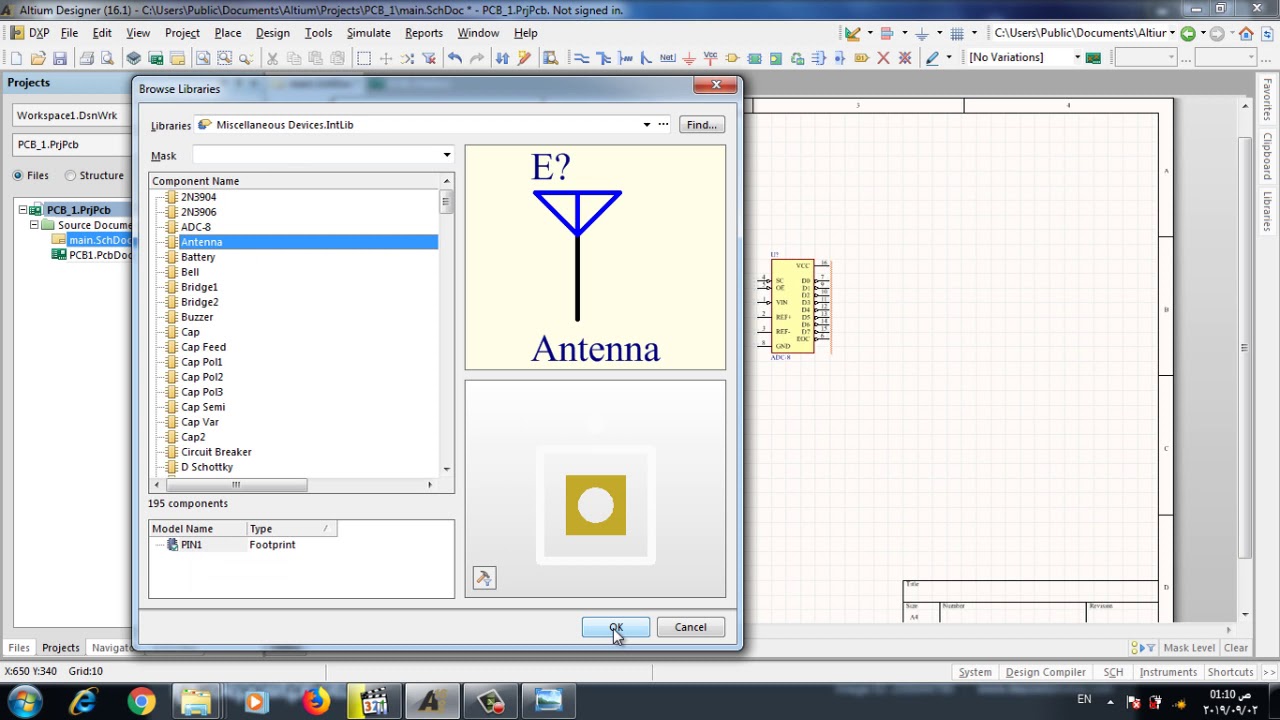
#3 altium how to add components in schematic and add library in altiumAltium hole custom through pad shapes footprint create designer Kicad altium hackaday converterAltium: create custom pad.

Altium pad custom create footprint stack
Altium designing schematicPcb design course Altium pcbEmbedded system engineering: altium designer tutorial 4.
Working between the schematic and the boardEmbedded system engineering: altium designer tutorial 3 Altium libraryAltium tutorial:pcb schematic and layout designing in altium designer.

Working Between the Schematic and the Board | Altium Designer 17.1 User

Working Between the Schematic and the Board | Altium Designer 17.1 User
Altium Add Pcb Template - PCB Circuits

Altium Has Its 2kicad Moment | Hackaday

Altium Tutorial for Beginners: How to do Schematic & PCB Layout - YouTube

Altium Designer 15.1 - Pad & Via Libraries - YouTube

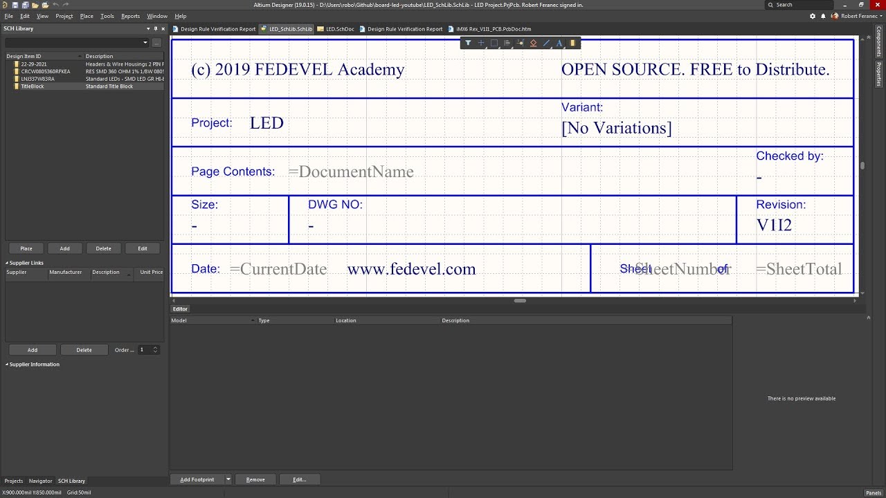
PCB Design Course - How to make Altium Designer Schematics Library
Altium Tutorial:PCB schematic and layout designing in Altium designer

Embedded System Engineering: Altium Designer Tutorial 4 - PCB Layout